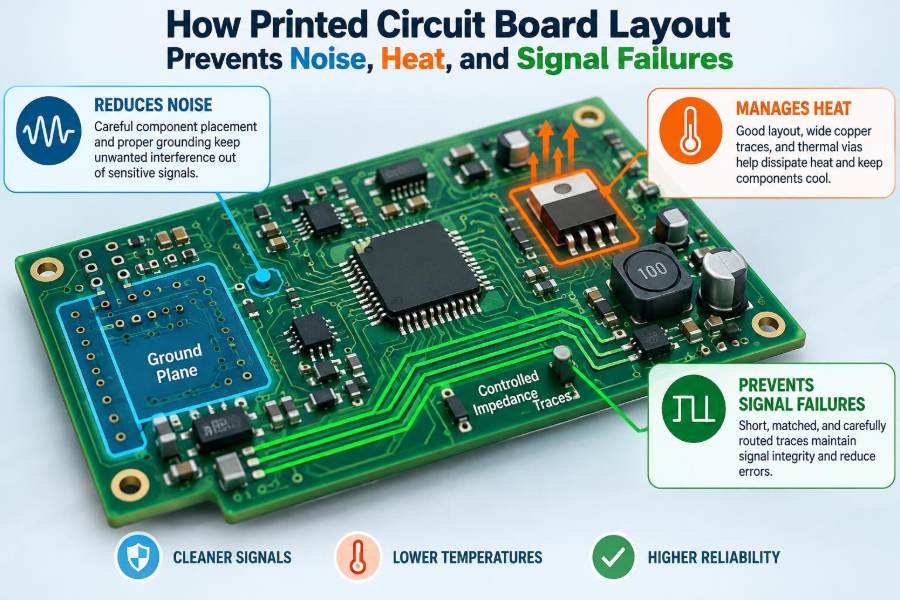

A prototype can power up, run a basic test, and still fail the moment its radio transmits, its motor starts, or its processor switches at full speed. The schematic may be correct. The components may be high quality. Yet the product resets, measures the wrong voltage, radiates too much interference, or slowly overheats.
Very often, the missing engineering work is in the printed circuit board layout. A PCB is not merely a place to connect symbols with copper tracks. It is part of the electrical circuit, part of the thermal system, and, at high frequencies, part of the electromagnetic environment.
Every trace has resistance, inductance, capacitance, and a path for return current. Every component placement decision changes current loops, heat flow, coupling, and the ability to manufacture and test the board.
Good layout therefore prevents problems before they appear in a lab or in the field. It turns a valid circuit diagram into a reliable physical system. ⚡
🧩 1. A PCB Layout Is a Physical Circuit
A schematic describes intended connections. A layout determines the real electrical behavior of those connections. A copper trace has length, width, thickness, nearby conductors, and a relationship to reference planes, all of which affect circuit performance.
At low frequency and low current, these effects may be small enough to ignore. As edge rates become faster, currents increase, and analog signals become smaller, physical geometry becomes a design variable.
The board is not an implementation detail after the circuit is designed; it is part of the design.
📐 2. Start with Constraints, Not Random Placement
Before moving footprints, collect the requirements that control the board shape and stackup. These include enclosure dimensions, connector locations, mounting holes, voltage and current levels, environmental conditions, safety spacing, assembly method, and test access.
Also identify circuits that need special treatment: switching converters, clocks, oscillators, high-speed interfaces, precision analog front ends, sensors, antennas, and high-current outputs.
- Define board outline and mechanical keep-out areas.
- Choose the layer count and tentative stackup early.
- List critical nets and their electrical requirements.
- Set manufacturable trace, spacing, via, and pad rules.
This preparation avoids the common mistake of discovering that a critical route has no practical path after the board is nearly complete.
🗺️ 3. Build the Stackup Around Reference Planes
A multilayer PCB stackup defines the order of copper and dielectric layers. Its most important purpose is often to place signal layers close to solid reference planes, typically ground planes.
A nearby plane gives return current a short path and creates predictable trace impedance. It also reduces loop area, which lowers radiation and susceptibility to external electromagnetic fields.
For many digital boards, an inner solid ground plane is more valuable than adding many fragmented copper pours. Routing fast signals adjacent to a continuous plane is a strong starting point.
🌊 4. Understand Return Current Before Routing Signals
Current always completes a loop. A signal trace carries outbound current, while return current flows through a reference conductor back to the source. On a board, high-frequency return current tends to travel directly beneath or near its associated trace on the closest continuous reference plane.
This behavior is not optional. If the intended return path is interrupted, the return current spreads out, finds another route, or crosses through capacitance between planes. The loop becomes larger and noisier.
Route the signal and protect its return path as one electromagnetic structure. This idea explains many otherwise mysterious layout rules.
✂️ 5. Never Route Critical Signals Across Plane Splits
A split or gap in a reference plane can force return current away from its natural path. Routing a fast clock, data line, or converter switch node across that gap creates a large loop area and can increase ringing, emissions, and crosstalk.
If a signal must change reference planes, provide a deliberate return path. Nearby ground stitching vias can connect ground planes and give the return current a short transition route.
Plane partitions are sometimes useful for specific safety or power purposes, but they require a clear understanding of every signal that crosses them. A continuous ground reference is usually the safer default.
📦 6. Place Components by Current Flow
Place parts according to how energy and signals move through the circuit, not simply by visual symmetry. Input connectors, protection components, filters, regulators, loads, processors, and outputs should form understandable functional paths.
For example, an input power connector should lead first to protection and bulk capacitance, then to conversion stages, and finally to distributed loads. A sensor connector should lead into protection and filtering before reaching a sensitive amplifier or converter.
Thoughtful placement shortens important connections and reduces the number of compromises required during routing.
⚡ 7. Keep High di/dt Loops Extremely Small
The most troublesome layout regions often contain rapidly changing current, described as high di/dt. Switching regulators, motor drivers, half bridges, and digital output stages can all generate these current changes.
Parasitic inductance produces voltage according to V = L × di/dt. Even a short trace can create significant voltage spikes when current changes quickly. These spikes cause ringing, stress components, and inject noise into nearby circuits.
Identify the compact loop that carries switching current, then place its components so that loop is physically tight. Do not allow this loop to wander around the board.
🔋 8. Place Decoupling Capacitors at the IC Power Pins
A decoupling capacitor supplies short bursts of current when an integrated circuit changes state. Its effectiveness depends far more on its connection inductance than on its label or nominal capacitance alone.
Place each local capacitor close to the relevant power pin, with a short path to the power connection and an equally short path to ground. A ground via near the capacitor pad is often better than a distant route to ground.
Bulk capacitors serve a different role: they support lower-frequency load changes and stabilize power entry points or regulator stages. Both local and bulk capacitance matter, but they should not be treated as interchangeable.
🔄 9. Lay Out Switching Regulators as Power Loops
A switching converter is a power circuit with fast edges, not just a regulator IC plus a few passive parts. The input capacitor, switching device or IC, inductor, diode or synchronous switch, and output capacitor must be arranged around the converter topology.
The input capacitor is especially important because it supplies pulsed input current. Place it tightly between the converter input and ground connections. Keep the switch node copper compact because it is often electrically noisy.
Follow the controller manufacturer’s recommended layout as a starting point, then verify that the high-current and high-frequency loops remain compact on the actual board.
🧱 10. Use Ground Planes Intentionally
A ground plane lowers impedance, supports return current, improves shielding, and spreads heat. However, a ground plane works best when it is continuous and connected by many low-inductance paths where needed.
Thin ground traces can create unwanted shared impedance. When multiple circuits share a narrow return conductor, voltage drops from one circuit can appear as noise in another. A plane reduces this risk by offering many parallel paths.
Do not assume every copper area labeled ground is equally useful. Narrow necks, isolated islands, and slots can limit return current and undermine the purpose of the plane.
🎯 11. Separate Noisy and Sensitive Functional Areas
Board zoning is a practical way to reduce coupling. Put noisy power conversion, high-current drivers, and fast digital interfaces away from sensitive analog inputs, reference circuits, antennas, and low-level sensors.
Separation is not the same as blindly splitting ground. Often the best strategy is to keep a solid common ground plane while controlling where currents flow through component placement and routing.
Place sensitive circuitry where it has a quiet reference and short connections to the signals it measures. Keep switching nodes and fast current loops outside that area.
🎙️ 12. Protect Precision Analog Signals
Small analog signals are easily disturbed by electric fields, magnetic fields, ground noise, leakage, and digital switching. The layout of an amplifier or analog-to-digital converter input can matter as much as the amplifier’s datasheet specifications.
Keep high-impedance nodes short, clean, and away from noisy traces. Place input filters and protection components near the connector or source. Put the amplifier and its feedback components close together to minimize pickup.
For converters, keep the analog input network, voltage reference, and local decoupling arranged as a compact subsystem. Route digital clocks and outputs away from these sensitive nodes.
🕰️ 13. Treat Clocks as High-Frequency Sources
A clock may have a modest repetition frequency but very fast rising and falling edges. Those edges contain higher-frequency energy and can excite transmission-line effects, reflections, and radiation.
Keep oscillator-to-IC connections short. Avoid stubs, unnecessary vias, and nearby aggressive signals. Crystal load capacitors should have short, symmetric connections to the crystal pins and a quiet return path.
Do not route clock traces over gaps in their reference plane. A stable reference plane makes clock behavior more predictable and reduces the chance that the clock becomes an antenna.
🚦 14. Know When a Trace Is a Transmission Line
A trace behaves like a transmission line when signal travel time becomes significant compared with edge transition time. The exact threshold depends on the interface, stackup, driver, and receiver, so treating only very high data-rate signals as transmission lines is unsafe.
Transmission lines have characteristic impedance. Sudden changes in width, reference plane distance, vias, connectors, and stubs create discontinuities that can reflect energy.
Controlled impedance routing becomes important for interfaces with defined impedance requirements. The fabricator’s actual stackup, not a generic calculator assumption, should guide width and spacing choices.
🪞 15. Reduce Reflections with Clean Topology
Reflections occur when a fast signal encounters an impedance change. The receiver may see overshoot, undershoot, multiple threshold crossings, or timing uncertainty. These effects can cause intermittent digital failures that are difficult to reproduce.
Use a routing topology appropriate to the interface. Point-to-point signals usually benefit from a direct route with minimal stubs. Multi-drop buses need deliberate termination and branch management.
Common approaches
- Series termination: a resistor near the driver that slows the launched edge.
- Parallel termination: a resistor network near the receiver that matches the line but consumes DC power in many cases.
- AC termination: a frequency-dependent option used for selected signal types.
Termination should be chosen from signal behavior and interface guidance, not added automatically.
🤝 16. Control Crosstalk Between Nearby Traces
Crosstalk is unwanted coupling from one signal path into another. It can occur through electric fields between conductors or magnetic fields around current loops. Long parallel runs are a common cause.
Keep sensitive traces away from fast aggressors, especially clocks, switch nodes, and high-current paths. Increase spacing where possible, shorten parallel overlap, and use a close reference plane to confine fields.
For some critical routes, a grounded guard trace with frequent stitching vias may help, but it is not a universal cure. Good spacing and a continuous reference plane are usually more fundamental.
↔️ 17. Route Differential Pairs as Coupled Systems
Differential signaling depends on the relationship between two conductors. The pair should remain close enough to maintain intended coupling, travel over the same reference environment, and avoid unnecessary asymmetry.
Keep the traces similar in length when the interface requires timing matching, but do not add excessive serpentine routing without need. Tight, unnecessary meanders can increase coupling and create local discontinuities.
When changing layers, use a symmetric via arrangement where practical and maintain a nearby reference transition. Preserve the pair’s impedance and return path through the whole route.
🌡️ 18. Design Copper for Heat Flow
Heat travels from a component junction through its package, pads, copper, vias, dielectric layers, and eventually into surrounding air, an enclosure, or a heatsink. Layout affects several steps in this path.
Use sufficient copper area for power devices and regulators, but remember that copper connected to a small thermal pad may require thermal relief decisions that balance solderability with heat transfer. Large exposed-pad packages often rely on a carefully designed thermal land.
Thermal design begins with estimating dissipation and identifying the hottest components. It should not be postponed until after all routing is finished. 🌡️
🕳️ 19. Use Thermal Vias Correctly
Thermal vias conduct heat from a component’s copper pad or thermal area to inner and opposite-side copper planes. An array of small vias beneath an exposed pad can substantially improve the path into the board.
Via design must match the assembly process. Open vias in a solderable pad can wick solder away during reflow unless the fabrication and assembly approach accounts for them.
Connect thermal vias to broad copper regions that can actually spread heat. Vias leading only to small isolated shapes offer less benefit than vias tied into useful internal planes.
🔥 20. Keep Heat Away from Temperature-Sensitive Parts
Hot components can distort measurements long before they create a reliability concern. Voltage references, precision resistors, temperature sensors, batteries, electrolytic capacitors, and some oscillators can all be affected by local temperature rise or airflow.
Place heat-generating components away from precision sensing areas. Consider the direction of natural convection in the intended product orientation, as warm air can carry heat across the board.
Thermal isolation slots or narrow copper connections may help certain sensors, but they must be evaluated against mechanical strength, return-current continuity, and manufacturability.
🛤️ 21. Size Power Traces for Current and Voltage Drop
Power routing must handle steady current, transient current, allowable temperature rise, and voltage drop. A trace that survives electrically may still cause a low-voltage device to malfunction if the load sees too much drop during a current burst.
Use wide traces, copper pours, or planes for significant current paths. Keep supply and return paths both low impedance; improving only the positive conductor does not complete the solution.
Pay special attention to connectors, fuses, current-sense resistors, vias, and narrow necks. These are often the real bottlenecks in a power path.
🧭 22. Route Current-Sense Connections with Kelvin Technique
A current-sense resistor develops a small voltage that may be measured by a sensitive amplifier. If the measurement traces share the high-current copper path, resistive drops in that copper become part of the reading.
Use separate, low-current sense traces from the resistor’s pads to the measurement input. This arrangement is commonly called a Kelvin connection.
Keep the sense pair away from switching nodes and route it as a quiet differential measurement path when appropriate. The power path should carry load current; the sense path should report voltage, not carry power.
🛡️ 23. Put Protection at the Entry Point
Electrostatic discharge, cable transients, and other external disturbances enter through connectors. Place protection devices close to the entry point so the transient current can be diverted before it travels across the board.
The path from connector to protection device and then to its return plane must be short and low inductance. A protection component placed far from the connector can allow the disturbance to travel through vulnerable circuitry first.
After protection, add filtering or conditioning as required by the interface. Treat connector regions as boundaries between the outside world and the controlled board environment.
📡 24. Give RF and Antennas a Quiet Environment
RF layout is especially sensitive to geometry because traces, pads, vias, ground shapes, and nearby objects affect impedance and radiation. Follow the module, antenna, and connector guidance for keep-out areas and ground requirements.
Keep switching converters, clocks, displays, metal hardware, and noisy cables away from antennas. Avoid copper, traces, or components in an antenna keep-out region unless the antenna documentation explicitly allows them.
A radio can fail because of receiver desensitization even when its transmitted signal appears functional. The entire board’s noise environment matters.
🏭 25. Design for Manufacturing, Assembly, and Test
A reliable electrical layout must also be buildable. Use spacing, annular ring, drill, solder-mask, and copper-clearance rules that the selected fabricator can consistently produce. Confirm the process capability instead of relying on minimum values from an unrelated board house.
Provide sensible component spacing for placement and soldering. Keep polarized markings visible where possible, orient similar parts consistently, and leave access for programming connectors and test points.
- Ensure test points are reachable by probes or fixtures.
- Avoid placing tall parts where they block assembly tools.
- Check that connectors mate within enclosure clearances.
- Consider how the board will be inspected and reworked.
Manufacturing constraints are design inputs, not final-stage obstacles.
🔍 26. Review the Layout in Several Different Ways
Design-rule checking is essential, but it cannot determine whether a switch node is too large or whether an analog return path is polluted. A strong review combines automated checks with circuit-aware inspection.
Useful review passes
- Connectivity: Are all nets and pins correctly connected?
- Return paths: Does every fast signal have a continuous nearby reference?
- Power loops: Are high di/dt loops compact?
- Thermal paths: Can heat reach copper and escape the board?
- Mechanical fit: Do board, connectors, screws, and enclosure coexist?
Review with the schematic visible. Looking only at artwork makes it easier to miss the intended function of each connection.
🧪 27. Validate the Finished Board with Measurements
Layout quality should be verified on hardware. Measure supply ripple at the load with probing methods that minimize probe-ground inductance. Inspect switch-node ringing, clock integrity, temperature rise, analog noise, and behavior during load transients.
When a problem appears, examine current loops and return paths before changing component values at random. A capacitor, resistor, or ferrite bead may help, but it cannot always compensate for a large inductive loop or a broken reference path.
Document what worked and what did not. Each board revision can become a practical library of layout knowledge for future designs.
✅ 28. The Core Principle: Control Energy Paths
PCB layout prevents failures by controlling where electrical energy flows. For noise, control fast current loops, return paths, field coupling, and reference continuity. For heat, control the conduction path from hot devices into copper, vias, and the surrounding system.
For signal integrity, control impedance, topology, discontinuities, and timing relationships. For reliable power, control resistance, inductance, current density, and voltage drop.
The most dependable layouts make every important path short, intentional, continuous, and appropriate for the energy it carries.
A board that looks orderly is not automatically robust, but a robust board is usually organized around physical behavior rather than cosmetic routing. Think in loops, return paths, fields, and heat flow, and PCB layout becomes a powerful method of preventing failure before it reaches the bench. ⚡🔬🛠️